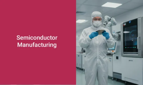
This comprehensive training program provides a systematic and detailed exploration of semiconductor manufacturing, covering the entire integrated circuit production journey from raw silicon to packaged chips. The program incorporates global industry standards, best practices, and cutting edge technologies that define modern semiconductor fabrication. Participants will gain deep insights into the fundamental physics and chemistry underlying semiconductor devices, the sophisticated processes used in wafer fabrication, and the advanced control and diagnostic techniques essential for achieving high yields in high volume manufacturing environments.
The program is built around the concept of manufacturing as defined by the transformation of raw materials into finished products, with specific emphasis on the unique challenges of semiconductor production where hundreds of sequential process steps must be performed with near perfection. The training draws extensively from internationally recognized guidelines including the Environmental, Health, and Safety Guidelines for Semiconductors and Other Electronics Manufacturing published by the World Bank Group, as well as industry standards from organizations such as SEMI and the International Technology Roadmap for Semiconductors. These references ensure that the program reflects good international industry practice as defined by skilled and experienced professionals engaged in semiconductor manufacturing under similar circumstances globally.
Participants will explore the entire manufacturing ecosystem, from the historical evolution of semiconductor processing to the latest advancements in extreme ultraviolet lithography, gate-all-around transistors, and artificial intelligence driven process control. The program emphasizes both theoretical understanding and practical application, enabling learners to communicate semiconductor manufacturing concepts effectively and to apply their knowledge in real-world production environments. The curriculum is structured to accommodate learners with diverse backgrounds, providing foundational knowledge while progressively building expertise in advanced topics.
The primary objectives of this training program are:
Learning Outcomes
Upon successful completion of this program, participants will be able to:
The scope of this training program encompasses the complete semiconductor manufacturing value chain, organized into thirty comprehensive modules covering:
Global References and International Standards
| Reference/Standard | Source | Relevance |
| Environmental, Health, and Safety Guidelines for Semiconductors and Other Electronics Manufacturing | World Bank Group | Good International Industry Practice (GIIP) for environmental and safety performance |
| International Technology Roadmap for Semiconductors | ITRS | Technology trends and process benchmarks |
| ISO 14001 Environmental Management Systems | International Organization for Standardization | Environmental compliance and sustainability |
| ISO 45001 Occupational Health and Safety | International Organization for Standardization | Worker health and safety management |
| ISO 9001 Quality Management Systems | International Organization for Standardization | Quality assurance and continuous improvement |
| SEMI S2 Guideline for Equipment EHS | Semiconductor Equipment and Materials International | Equipment safety specifications and compliance |
| SEMI F5-90 Guide for Gaseous Exhaust Emissions | SEMI | Air emission monitoring and control |
| EU RoHS Directive 2002/95/EC | European Union | Restriction of hazardous substances in electronic equipment |
| EU WEEE Directive 2002/96/EC | European Union | Waste electrical and electronic equipment management |
| US EPA 40 CFR Part 63 Semiconductor Manufacturing | US Environmental Protection Agency | Hazardous air pollutant emission standards |
| Helcom Recommendation 23/7 | Helsinki Commission | Industrial wastewater management |
| German Technical Instructions on Air Quality Control (TA Luft) | German Federal Government | Air quality and emission control |
| German Waste Water Ordinance (AbwV) | German Federal Ministry for Environment | Wastewater discharge requirements |
Industry Alignment
This program is aligned with the needs of the global semiconductor industry and reflects the standards and practices of leading semiconductor manufacturers. The curriculum has been developed based on:
This program is designed for professionals and students seeking to develop comprehensive expertise in semiconductor manufacturing.
Entry Prerequisites
To ensure successful participation in this program, learners should possess:
Upon successful completion of this program, participants will be awarded a certification that validates their comprehensive understanding of semiconductor manufacturing processes and methodologies. The certification demonstrates competence in the following areas:
Semiconductor manufacturing is governed by a complex framework of international and regional regulations that ensure environmental protection, worker safety, and product compliance. The World Bank Group’s Environmental, Health, and Safety (EHS) Guidelines serve as foundational technical reference documents, establishing performance levels achievable by existing technology at reasonable cost. These guidelines align with Good International Industry Practice (GIIP) and are applied when projects involve World Bank Group members, with the general principle that projects must achieve the more stringent requirement when host country regulations differ.
Environmental Management Systems (EMS) are universally adopted by leading manufacturers. The ISO 14001 standard forms the backbone of environmental management, with industry leaders maintaining certifications across their global facilities. These systems focus on reducing greenhouse gas emissions, enhancing water recovery rates, and minimizing waste generation through source reduction and recycling. Occupational Health and Safety is governed by ISO 45001, the international standard that replaced OHSAS 18001, with major semiconductor companies achieving ISO 45001 certification across all their worksites, implementing robust health and safety management systems to prevent work-related injuries and illnesses.
The semiconductor industry has its own specialized safety standards, primarily the SEMI S2 Guideline for Environmental, Health, and Safety for Semiconductor Manufacturing Equipment. This globally recognized guideline addresses equipment safety specifications including electrical safety, mechanical hazards, chemical handling, fire protection, and radiation safety. The latest version incorporates key revisions related to high pressure systems, equipment decommissioning, flammable substances, and safety labeling.
Product Compliance Regulations include the EU Directive on Restriction of the Use of Certain Hazardous Substances (RoHS), which restricts lead, mercury, cadmium, chromium (Cr VI), and specific flame retardants. The semiconductor industry also faces increasing regulatory scrutiny on per- and polyfluoroalkyl substances (PFAS), with restrictions being considered under the Stockholm Convention on Persistent Organic Pollutants and emerging regulations in the US, Europe, and Asia.
Key Regulatory Frameworks and Standards
| Regulatory Framework | Scope and Purpose | Key Requirements |
| World Bank Group EHS Guidelines | Environmental, health, and safety performance levels for semiconductor manufacturing projects | Application of Good International Industry Practice (GIIP); achieving more stringent requirements when host country regulations differ |
| ISO 14001 | Environmental Management Systems | Greenhouse gas emission reduction; water recovery enhancement; waste minimization through source reduction and recycling |
| ISO 45001 | Occupational Health and Safety Management | Prevention of work-related injuries and illnesses; implementation of robust health and safety management systems |
| SEMI S2 Guideline | Equipment Environmental, Health, and Safety | Electrical safety; mechanical hazards; chemical handling; fire protection; radiation safety; high pressure systems; equipment decommissioning |
| EU RoHS Directive | Restriction of Hazardous Substances in Electrical and Electronic Equipment | Restriction of lead, mercury, cadmium, chromium (Cr VI), and specific flame retardants in electronic products |
| Stockholm Convention | Persistent Organic Pollutants (POPs) Management | Restrictions on PFAS and other persistent organic pollutants; manufacturing exemptions and phase-out strategies |
Key Regulatory Focus Areas
The program develops competencies across six domains:
| Domain | Key Competencies |
| Semiconductor Fundamentals | Explain semiconductor physics; understand device operation; apply doping concepts |
| Manufacturing Processes | Describe all unit processes; explain process integration; identify process parameters |
| Process Control and Monitoring | Apply SPC; understand process capability; implement control charts; diagnose faults |
| Yield and Quality Management | Model yield; analyze defects; implement improvement strategies; apply quality systems |
| Environmental and Safety Management | Understand regulations; implement EHS practices; manage hazardous materials |
| Emerging Technologies | Understand advanced lithography; GAA transistors; AI applications; future trends |

We provide training programs designed to help you meet quality and compliance standards. Our courses cover GMP, GLP, GCP, GEP, GDP, and Quality Assurance.